Intel Promotes EMIB for Larger AI Chips
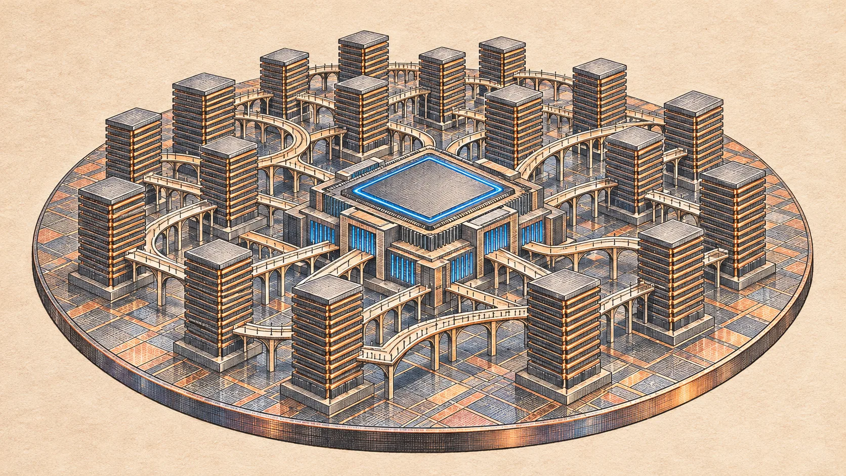
- •Intel says EMIB achieves over 90% wafer utilization, versus roughly 60% for interposer-based packaging
- •Google and Amazon are reportedly considering EMIB-T for future custom AI chips
- •Intel envisions packages with more than 70 bridges and over 32 HBM stacks
Intel is promoting its EMIB and EMIB-T advanced packaging technologies as alternatives while TSMC’s CoWoS capacity is tight, according to a TrendForce report citing ZDNet Korea and Economic Daily News. Intel Foundry Packaging Director Kyu-oh Lee said EMIB uses localized silicon bridges instead of a full-size silicon interposer, yielding more than 90% wafer utilization versus roughly 60% for interposer-based designs. EMIB-T adds through-silicon vias (vertical electrical connections through silicon) to the bridges to deliver power, the report said.
Industry sources cited by ZDNet Korea say Google’s TPU v9 lineup could use EMIB-T for both HumuFish and TriggerFish, while WhaleFish is expected to use TSMC’s CoWoS-L. Amazon is also reportedly planning to use EMIB-T in custom AI chips. The reported adoption remains prospective.
Lee said AI chips commercialized in 2026 have packages up to 120 × 120 mm, with 12 HBM stacks and more than 20 EMIB bridges. Chips in development target packages of at least 120 × 180 mm, 16 or more HBM stacks and at least 38 bridges. Intel envisions future packages measuring 240 × 240 mm, with over 32 HBM stacks and more than 70 bridges.
Taiwanese foundry UMC makes EMIB silicon bridges at fabs in Taiwan and Singapore using mature 12-inch wafer processes, Economic Daily News previously reported. Separately, TrendForce says TSMC’s CoWoS-L is expected to support a 5.5X reticle-size package with four chiplets and 12 HBM stacks in 2026, then scale to 14X by 2028, accommodating 20 chiplets and 20 HBM stacks.